
Samsung and Kioxia are simultaneously ramping mass production of PCIe 6.0 NAND storage, compressing the technology cycle for AI data centers.
Samsung and Kioxia are simultaneously ramping mass production of PCIe 6.0 NAND storage, compressing the technology cycle for AI data centers.
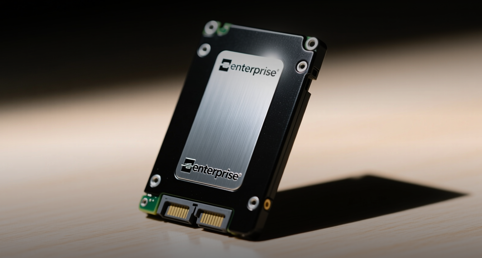
Samsung Electronics and Kioxia have begun mass production of PCIe 6.0 enterprise SSDs within weeks of each other, compressing the NAND technology cycle as AI data centers demand faster storage for inference workloads. Kioxia started volume output of its 10th-generation BiCS 10 NAND (332-layer stacking) at its Kitakami K2 fab in Iwate Prefecture in early July, while Samsung launched its PM1763 PCIe 6.0 eSSD built on ninth-generation V-NAND with a 4nm controller.
"As AI infrastructure evolves, storage must deliver not only higher performance but also greater efficiency and deployment flexibility," Neville Ichhaporia, senior vice president and general manager of the SSD business unit at KIOXIA America, said.
Kioxia's CM10 eSSD delivers up to 92 percent higher sequential read performance and about 85 percent higher random read performance than its predecessor, according to company data. The drive supports the NVIDIA CMX context memory storage solution, which extends effective GPU memory with a shared, pod-level context tier for KV cache. Available in E3.S, E1.S, and 2.5-inch form factors with capacities from 1.60TB to 61.44TB, the CM10 offers cold-plate liquid cooling capability in select form factors and read-intensive (1 DWPD) and mixed-use (3 DWPD) endurance options.
Samsung completed UFS 5.0 development in June and plans mass production in the fourth quarter, targeting 10.8GB/s bandwidth on ninth-generation V-NAND. Kioxia expects to begin UFS 5.0 output by year-end, with data processing speed roughly double that of UFS 4.1, pairing its in-house controller with eighth-generation NAND.
The simultaneous ramp compresses the commercialization window for new NAND specifications, with both companies shipping PCIe 6.0 products within the same quarter. Samsung held 31.6 percent of the global NAND market in the first quarter, followed by SK hynix at 17.6 percent and Kioxia at 13.9 percent, per TrendForce data. The race carries direct implications for AI infrastructure spending, where storage bottlenecks have constrained inference throughput.
Samsung's V10 NAND, estimated at more than 430 layers, introduces hybrid bonding and a three-stack architecture for the first time. The company completed internal production readiness approval and announced mass production launch this month, though initial output will be limited as equipment investment has not fully ramped, according to semiconductor industry sources cited by ZDNet. Samsung is also accelerating development of its 500-layer V11 generation and increasing shipments of its ninth-generation V-NAND to NVIDIA.
SK hynix, the second-largest NAND supplier, plans to begin mass production of its 375-layer 4D NAND by year-end, converting existing production lines at its M15 fab in Cheongju rather than building new capacity. The company will introduce molybdenum into part of its word-line metal gate electrodes, replacing selected tungsten layers to reduce resistance and enable higher-density NAND. SK hynix says the 375-layer generation improves performance per watt by 2.5 times over the previous generation, targeting AI data centers where power efficiency is a primary constraint.
The UFS 5.0 specification, entering commercialization this year, targets mobile NAND applications for on-device AI. Kioxia's UFS 5.0 solution pairs its in-house controller with eighth-generation NAND, while Samsung's version uses ninth-generation V-NAND. Both companies are targeting these products at AI smartphones and edge devices that require faster local storage for model inference, where data processing speed roughly doubles compared with UFS 4.1.
The broader AI storage push extends beyond PCIe and UFS. At the Flash Memory Summit in Santa Clara this week, Sandisk and SK hynix released the High Bandwidth Flash (HBF) technical specification through the Open Compute Project, defining a new memory tier for AI inference that sits between HBM and conventional storage. NVIDIA also announced it is open sourcing its cuFile APIs, which let GPUs read from and write to storage directly, reducing CPU involvement in data movement.
For investors, the accelerated NAND cycle favors suppliers with the deepest process technology and fastest time-to-market. Samsung's scale advantage in NAND (31.6 percent share) provides pricing power, while Kioxia's early 300-plus-layer production demonstrates technical parity. SK hynix's focus on power efficiency targets the data center segment where energy costs dominate. The compressed technology cycle could pressure margins for smaller NAND suppliers unable to match the pace of the top three, while hyperscalers stand to benefit from faster storage performance at competitive prices.
This article is for informational purposes only and does not constitute investment advice.
