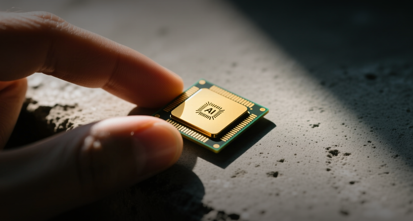
TSMC is adding three advanced chip packaging facilities at the Chiayi Science Park in Taiwan, responding to insatiable demand from AI chip customers including Nvidia and AMD.
Taiwan Semiconductor Manufacturing Co will build three additional advanced packaging plants in Phase II of the Chiayi Science Park, National Science and Technology Council Minister Wu Cheng-wen said Sunday at the groundbreaking ceremony. The roughly 90-hectare site will be developed into an advanced packaging industry cluster led by TSMC, with two facilities already in mass production at Phase I since last month.
"Phase II development of the Chiayi Science Park would strengthen the resilience of the regional economy and help transform Chiayi County into a global production hub for advanced semiconductor packaging," Wu said. Once both phases are operational, companies at the park are expected to generate more than NT$300 billion (US$9.35 billion) in annual output and create 9,000 jobs, he added.
The expansion targets growing global demand for high-performance computing chips and advanced packaging technologies, particularly TSMC's CoWoS (Chip-on-Wafer-on-Substrate) technology, which has become the standard for AI accelerators. Nvidia, AMD and Amazon Web Services are among the customers relying on CoWoS to package their most advanced chips, and demand has consistently outstripped supply for more than two years.
The AI packaging bottleneck
TSMC currently operates five advanced packaging and testing plants across Taiwan at sites including Hsinchu, Taichung, Tainan, Taoyuan and Miaoli. The Chiayi expansion will connect with other Southern Taiwan Science Park branches in Tainan, Kaohsiung and Pingtung, as well as the Central Taiwan Science Park and Hsinchu Science Park, to form what Wu described as the world's most comprehensive AI and semiconductor industry corridor.
The capacity crunch has created opportunities for competitors. Intel is positioning its EMIB (Embedded Multi-die Interconnect Bridge) technology as an alternative to CoWoS, and Taiwanese packaging and test companies including ASE Technology, SPIL, Powertech and KYEC are absorbing spillover orders that TSMC cannot fulfill. Reports have indicated Nvidia may move some advanced packaging orders to Intel for its next-generation Feynman GPUs, though Nvidia has not confirmed the shift.
TSMC is also building two packaging plants in Arizona as part of its 12-fab global expansion plan, reflecting a broader migration of semiconductor manufacturing to the US that DigiTimes reported in mid-2025 is accelerating cross-Pacific supplier expansion.
Investor implications
TSMC is scheduled to report second-quarter revenue Monday, with bottom-line figures due at an earnings conference Thursday. Yuanta Securities estimates Q2 revenue of NT$1.276 trillion, up 12.5 percent quarter-on-quarter and 36.7 percent year-on-year, with gross margin reaching 67.5 percent — the upper end of TSMC's guidance range — and earnings per share of NT$24.1.
The packaging expansion signals that TSMC expects AI chip demand to remain elevated for years. Nvidia shares trade at roughly 35 times forward earnings, and any easing of the CoWoS bottleneck could accelerate GPU shipments and revenue recognition for both companies. However, Intel's push into advanced packaging and the spillover benefits for ASE and other Taiwanese test houses introduce competitive dynamics that investors should monitor. TSMC's ability to maintain its packaging lead while scaling capacity will be a key determinant of its pricing power and margin trajectory through 2027.
This article is for informational purposes only and does not constitute investment advice.