
SEMICON Taiwan 2026 reveals AI semiconductor expansion shifting to the full backend chain, with TSMC's CoWoS capacity forecast at 260,000 wafers monthly by end-2027 and CPO testing emerging as the next constraint.
SEMICON Taiwan 2026 reveals AI semiconductor expansion shifting to the full backend chain, with TSMC's CoWoS capacity forecast at 260,000 wafers monthly by end-2027 and CPO testing emerging as the next constraint.
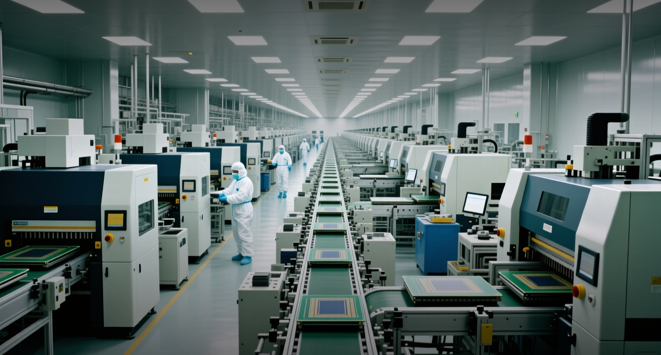
The AI chip buildout is extending beyond wafer fabs into advanced packaging, optical interconnect, and testing, with TSMC's CoWoS capacity forecast to reach 260,000 wafers per month by end-2027.
The shift reflects a structural imbalance that TSMC speakers laid out at SEMICON Taiwan 2026: AI computing capability grows roughly three times every two years while I/O transmission grows only 1.4 times over the same period. Chen Ming-Fa, deputy project director at TSMC, said at the Silicon Photonics International Forum that this widening gap makes optical interconnect essential to break through system-level communication bottlenecks, pushing the industry from front-end chip production toward full-chain backend expansion.
UBS raised its end-2027 CoWoS capacity forecast to 260,000 wafers per month as TSMC's 5.5x reticle CoWoS is already in mass production with yields above 98 percent. TSMC plans to expand to a 14x reticle by 2028 supporting 20-layer HBM stacks, and 24-layer HBM by 2029. TrendForce projects TSMC's CoWoS monthly capacity will reach 120,000 to 140,000 wafers within 2026, with OSAT partners adding another 50,000 to 60,000 wafers monthly, bringing total industry capacity near 200,000 wafers.
The expansion is spilling beyond TSMC's own fabs. UBS said TSMC appears cautious on its second-half 2027 CoWoS expansion pace, with some CoW outsourcing likely flowing to ASE. ASE Semiconductor Executive Vice President Hung Sung-Ching said the company is planning seven advanced packaging facilities in the Greater Kaohsiung area — four in Nanzih, two in Renwu, and one in Luzhu — to absorb the demand. Equipment lead times have extended to two years, and substrate and PCB supply remain tight, making backend capacity the new constraint on AI chip delivery.
TSMC's 3DFabric platform integrates SoIC 3D chip stacking, COUPE silicon photonics, and CoWoS advanced packaging. The number of AI computing transistors integrated into a single CoWoS package is projected to grow more than 48-fold from 2024 to 2029, with HBM bandwidth increasing 34-fold. The company's A14 logic process is targeting a 4.5-micrometer bonding pitch by 2029.
Panel-level packaging is also accelerating. UBS said equipment suppliers are gaining confidence in TSMC's CoPoS (310 by 310 millimeters) mass production, with the company targeting mid-2027 for process and equipment selection and 2028 for volume production.
On the optical interconnect front, TSMC's COUPE platform advances in three phases: COUPE on PCB targeting 1.6 Tbps OSFP optical modules, COUPE on Substrate integrated with CoWoS delivering 6.4 Tbps, and COUPE on Interposer targeting 12.8 Tbps optical engines directly integrated into processor packages. The company plans 200 Gbps per channel in 2026, rising to 400 Gbps by 2030.
As CPO moves from technology validation to mass production, the bottleneck is shifting from whether it can be done to whether it can be done reliably at scale. Citi's survey focused on active coupling and automated bonding in CPO manufacturing, which involves integrating EIC, PIC, lenses, and fiber/FAU components.
Nomura flagged testing as a critical constraint. Insertion 2 — the test step after EIC and PIC wafer bonding — currently has low throughput, prompting industry discussions about whether to skip it. Nomura said that while removing Insertion 2 shortens production cycles, some test coverage cannot be replicated downstream, so the step remains valuable for yield assessment and supply chain accountability.
UBS expects the industry to simplify Insertion 2 while increasing reliance on Insertion 3, which tests individual optical engines. Chroma ATE, the testing equipment maker, proposed a "shift-to-middle" approach: for high-density expansion switches, a defect in any single optical engine could scrap the entire CoWoS-level package, making 100 percent known-good verification at Insertion 3 a potential requirement for volume production.
TSMC Vice President Hsu Kuo-Chin warned that lasers, optical fibers, fiber connectors, and product testing are becoming the real bottlenecks for large-scale optical deployment. Silicon photonics is expected to exceed 50 percent market share by 2027, with optical transceiver sales growing 25 percent in 2025 and another 50 percent expected in 2026.
For investors, the backend expansion cycle favors TSMC (2330.TW), ASE, and testing equipment suppliers such as Chroma ATE. Equipment lead times stretching to two years signal sustained demand, while the shift toward 3D system integration and optical interconnect extends the AI semiconductor capex cycle into packaging, photonics, and testing segments that were previously secondary to wafer production.
This article is for informational purposes only and does not constitute investment advice.
