


Google's internally-developed Frozen chip aims to lower AI inference costs, challenging Nvidia's dominance in data center processors.
Google's internally-developed Frozen chip aims to lower AI inference costs, challenging Nvidia's dominance in data center processors.
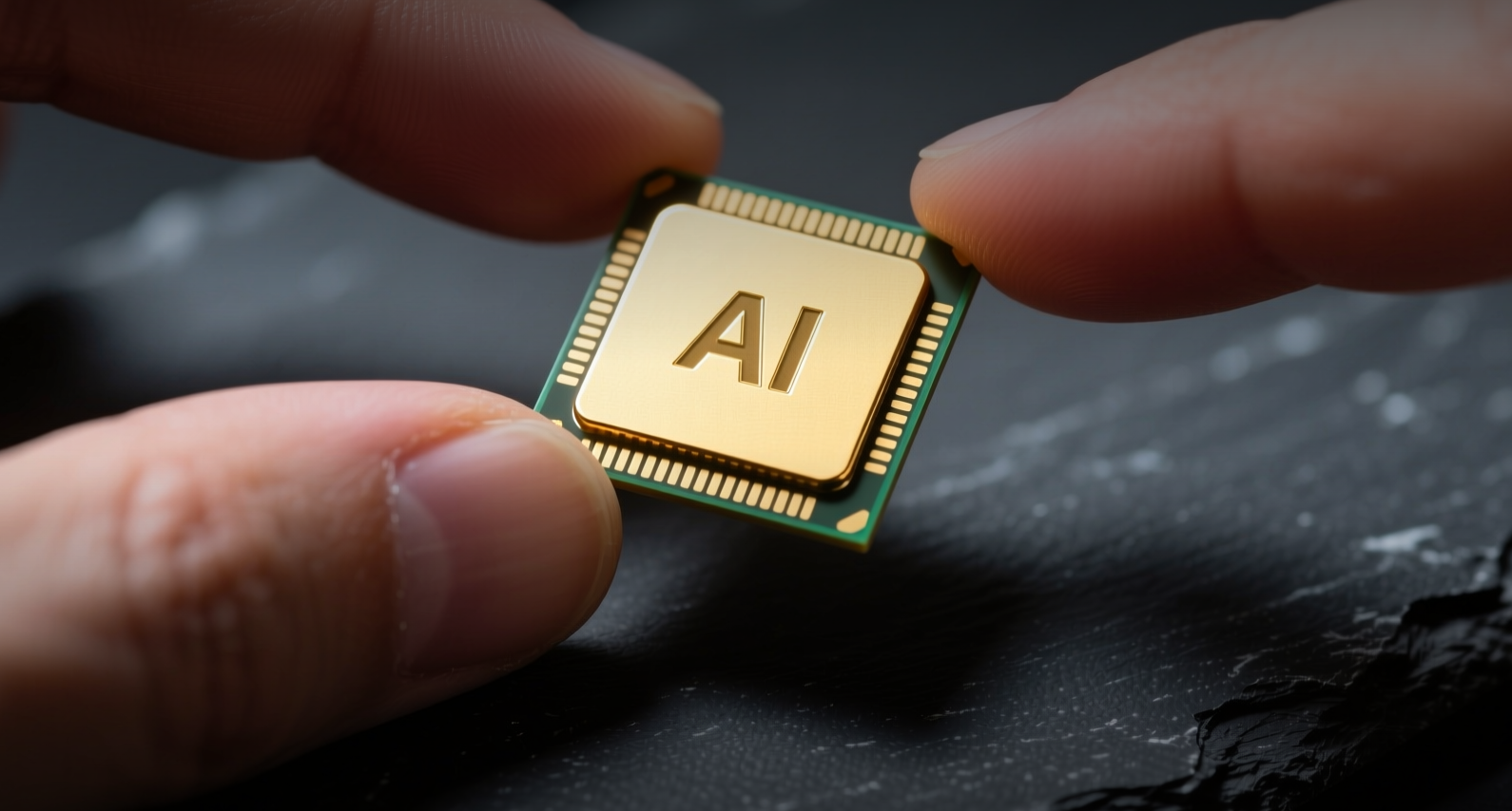
Google's internally-developed Frozen chip aims to lower AI inference costs, challenging Nvidia's dominance in data center processors.
Google's new chip, codenamed Frozen, is designed to run the company's AI models at significantly higher efficiency, threatening Nvidia's hold on the data center GPU market, according to a person familiar with the plans.
"We designed Frozen specifically for our inference workloads, targeting a meaningful improvement in performance per watt," a Google spokesperson said, declining to disclose technical specifications or a production timeline.
The chip will power Google's own AI models, including Gemini, reducing the company's reliance on external suppliers such as Nvidia. Google has not disclosed the process node, memory configuration, or performance benchmarks for Frozen. The company's previous in-house efforts include the Tensor Processing Unit, now in its fifth generation, and the Axion Arm-based server CPU announced in 2024. The TPU line has been a cornerstone of Google's AI infrastructure since 2015, with each generation delivering roughly 2x performance gains over its predecessor.
Alphabet shares rose on the news, reflecting investor optimism that in-house silicon could lower the company's AI infrastructure costs. Nvidia faces growing competition as hyperscalers including Amazon, with its Trainium and Inferentia chips, and Microsoft, which is developing its own Maia AI accelerator, push to reduce dependence on external GPU suppliers. The trend toward vertical integration in AI hardware has accelerated over the past two years as the cost of purchasing Nvidia GPUs has surged amid supply constraints.
Custom Silicon Arms Race
The Frozen chip represents Google's latest push to control its AI hardware stack. By designing chips tailored to its own neural network architectures used in search, advertising, and cloud services, Google can optimize for cost and performance in ways that general-purpose GPUs cannot match. The company's TPU strategy has already demonstrated the benefits of custom silicon: Google deployed TPUs across its data centers years before rivals developed comparable in-house alternatives, giving it a cost advantage in running large-scale AI workloads.
Google has not provided a timeline for Frozen's deployment or disclosed which foundry will manufacture the chip. The company's TPUs are manufactured by Broadcom using TSMC's process technology, and analysts expect a similar arrangement for Frozen. TSMC's advanced packaging capacity, particularly CoWoS (chip-on-wafer-on-substrate), remains a bottleneck for AI chip production across the industry, with lead times stretching beyond six months for some customers. Any delay in securing packaging capacity could push Frozen's deployment into late 2026 or early 2027.
Investment Implications
If Frozen delivers meaningful efficiency gains, it could pressure Nvidia's data center business and reshape competitive dynamics in cloud AI, where Google Cloud trails Amazon Web Services and Microsoft Azure but has invested heavily in AI capabilities. Alphabet trades at roughly 22x forward earnings, and lower infrastructure costs could provide a margin tailwind in coming quarters. The broader shift toward custom AI silicon has already eroded Nvidia's near-monopoly: Amazon's Inferentia chips now power parts of AWS, while Microsoft's Maia accelerator targets Azure workloads. For Google, the Frozen chip represents not just a cost-saving measure but a strategic imperative to maintain competitiveness in an AI landscape where hardware differentiation increasingly determines model performance and pricing.
This article is for informational purposes only and does not constitute investment advice.
