
Key Takeaways: Samsung's zHBM architecture stacks high-bandwidth memory directly atop AI accelerators, claiming eight times the performance of HBM5.
Key Takeaways: Samsung's zHBM architecture stacks high-bandwidth memory directly atop AI accelerators, claiming eight times the performance of HBM5.
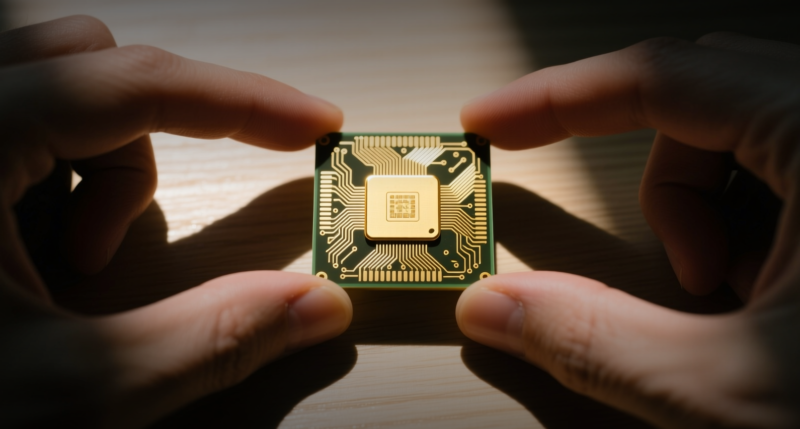
Samsung Electronics unveiled a 3D memory architecture that vertically stacks high-bandwidth memory atop AI accelerators, claiming eight times the performance of HBM5, as the chipmaker races SK Hynix and Micron for dominance in the AI memory market.
Samsung Memory executives Jin-Yub Lee, executive vice president and head of flash product and technology, and Kyungryun Kim, vice president and DRAM design project leader, presented the roadmap in a keynote titled "Driving the Wave of AI Revolution: 3D Innovations in Memory & Storage Architecture" at the Future of Memory and Storage conference in Santa Clara, California.
The zHBM concept model stacks HBM directly above AI accelerators rather than alongside them, cutting the distance data travels between processor and memory. Samsung claims the architecture delivers roughly eight times the performance of HBM5, more than 10 times the memory density, threefold energy efficiency gains, and thermal resistance reduced by more than half. The company also unveiled V10 BV-NAND, its first NAND built on wafer bonding technology with more than 400 layers, delivering a 58 percent density increase over the V9 generation.
The announcements come as Samsung seeks to close the gap with SK Hynix, which dominates the HBM market with Nvidia as its anchor customer. Samsung began mass production of HBM4 in February using its 1c DRAM and 4-nanometer base die, and shipped HBM4E samples in May. As the world's only integrated device manufacturer spanning memory, foundry, and advanced packaging, Samsung is using its turnkey model as a differentiator for AI infrastructure customers.
zHBM Claims 8x HBM5 Performance with Vertical Stacking
The zHBM architecture moves beyond conventional designs where HBM sits alongside the AI processor on the same substrate. By stacking memory vertically above the accelerator, Samsung aims to minimize data travel distance, which it says enables higher bandwidth and improved power efficiency for large-scale AI training and inference workloads.
Samsung says zHBM also supports customer-specific designs, allowing customized IP to be integrated into the interlayer between memory and the AI accelerator. This could expand memory capacity and enhance accelerator performance for hyperscalers building custom silicon — a segment where Nvidia, AMD, and Google have all invested heavily. The company plans to optimize AI processor and memory integration through zHBM in close collaboration with customers, though it did not disclose a production timeline or test conditions for its performance claims.
V10 BV-NAND Adds 58% Density with Wafer Bonding
Samsung's V10 BV-NAND marks the first use of wafer bonding technology in its NAND architecture, stacking memory cells to increase density by approximately 58 percent over V9. The announcement comes 13 years after Samsung introduced the industry's first V-NAND at the 2013 Flash Memory Summit. The company said the new architecture also improves read, write, and I/O performance, supporting high-capacity storage for AI systems.
The company also introduced zNAND-O, a high-performance NAND solution in development in four- and eight-layer versions, optimized for edge AI environments requiring real-time data processing. Samsung's broader portfolio showcased at FMS includes LPDDR5X-PIM, the industry's first LPDDR memory with processing-in-memory technology, and enterprise storage solutions PM1763 and BM1773, alongside roughly 30 memory and storage technologies on display.
The HBM market has become the central battleground for AI memory supremacy. SK Hynix has held the lead since Nvidia selected its HBM3 for the A100 and H100 accelerators, and the company's HBM4 is already in production. Micron has also secured design wins with its HBM3E, though it trails both Korean rivals in market share. Samsung's zHBM concept, if realized, could change the competitive calculus by integrating memory directly into the accelerator package — a move that would require close collaboration with chip designers like Nvidia, AMD, and custom silicon developers at Google and Amazon.
The AI memory market is one of the fastest-growing segments in semiconductors. SK Hynix shares rose 5 percent on Monday after six brokerages launched coverage with bullish ratings, citing its dominance in the AI memory market. Samsung's aggressive roadmap points to intensifying competition for HBM contracts with hyperscalers. Its IDM advantage — combining memory, foundry, and advanced packaging — could help it win custom AI accelerator deals that pure-play memory makers cannot serve. However, zHBM remains a concept model, and the company has not yet specified when it will move to production.
This article is for informational purposes only and does not constitute investment advice.
