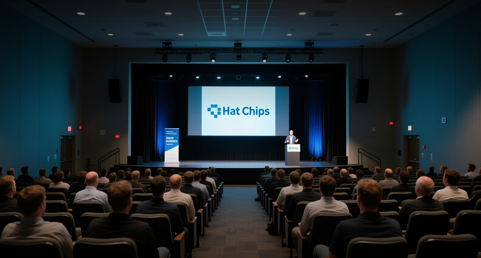
Samsung's three-stage HBM roadmap ends with zHBM, a true 3D architecture that stacks DRAM directly on compute chips and eliminates the interposer.
Samsung Electronics unveiled a three-stage high-bandwidth memory roadmap at the Hot Chips conference that culminates in zHBM, a 3D architecture stacking DRAM directly atop GPUs and TPUs, claiming a 70 percent power reduction and 230 percent bandwidth gain over HBM4E. The plan repositions the HBM base die from a passive data relay into a compute-capable partner, a shift that could reshape how AI accelerators are designed and who captures value in the memory stack.
"By mastering advanced packaging and unified SoC-DRAM co-design, we will break through the power, area, and capacity bottlenecks constraining AI systems," Sangwook Han of Samsung's DRAM design team said in his presentation.
The roadmap's first stage applies Samsung's D1c and 4nm logic processes to the HBM4 base die, replacing the traditional PHY with a die-to-die interface and offloading the memory controller from the compute chip. Samsung says that frees 5 to 10 percent of xPU silicon area for a 10 to 20 percent performance gain, while a Heat Path Block cuts peak temperatures by more than 35 percent. Stage two, dubbed AHBM, integrates memory expansion controllers and processing elements onto the base die to handle growing KV-cache demand. Stage three delivers zHBM, which Samsung says saves 100W per DRAM module and frees 8.3 percent of GPU power headroom, targeting I/O power of about 0.5 pJ/bit through wafer-on-wafer and hybrid cube bonding.
The plan lands as HBM supply tightens across the industry. Micron and SK Hynix have essentially sold out capacity through 2027, and Nvidia has told hyperscalers that AI server prices are rising more than 15 percent on memory costs, according to Bloomberg. Micron's Raghu Sriramaneni warned at the same conference that roughly 90 percent of semiconductor area in the latest AI packages is memory, consuming three times the wafer volume of standard DRAM.
The base die becomes a co-processor
HBM splits its work between stacked DRAM core dies, or C-dies, and a base die, or B-die, that carries the PHY and through-silicon vias linking to the compute chip. Current HBM4 stacks exceed 3TB/s of bandwidth, with HBM4E pushing toward 4TB/s and HBM5 doubling that to more than 60GB of capacity. Bandwidth growth now hits two hard limits: the physical ceiling on TSV count and pitch, and the I/O speed of the PHY inside the base die.
Samsung's answer is to make the base die do more. Moving the memory controller off the xPU, then adding processing elements, turns the B-die into a co-processor that offloads work from the accelerator. SK Hynix is taking a parallel path, positioning hybrid bonding as the route to 20-or-more-high stacks and pushing bump pitch below 18 micrometers, while Micron began mass production of its sixth-generation HBM4 at 2.8TB/s per stack for Nvidia's Vera Rubin platform.
The competitive stakes are visible in the challengers. Startup d-Matrix unveiled Raptor, a 3D-DRAM inference chip claiming 10 times the bandwidth of HBM4, with working test silicon behind it. Samsung's zHBM, however far off, points the same direction: stacking compute directly on DRAM and removing the interposer that dominates today's 2.5D packaging.
What it means for investors
Samsung's disclosure intensifies a three-way race with SK Hynix and Micron for AI accelerator memory supply, a market where Deloitte estimates memory now accounts for roughly one-fourth of the bill of materials on high-end AI server racks. If zHBM's power and bandwidth claims hold, Samsung's memory division could capture share in a segment where capacity is sold out through 2027 and supply tightness may persist beyond 2030, per SK Hynix management. Samsung did not disclose a timeline for zHBM production, and the architecture remains a roadmap rather than a shipping product, so near-term revenue impact is limited. The immediate read for investors is that memory, not compute, is becoming the binding constraint on AI system cost and performance.
This article is for informational purposes only and does not constitute investment advice.